
Samsung Electronics ha reso noto, mediante il comunicato stampa di seguito allegato, di aver sviluppato, presso i suoi centri di ricerca, una nuova tecnologia - indicata con la terminologia di "Through Silicon Via" (TSV) - che promotte non poche innovazioni nel campo delle memorie DRAM dal momento che permetterà, in accordo al produttore, di conseguire il duplice obiettivo legato all'incremento delle prestazioni, da un lato, e alla riduzione del consumo di potenza dall'altro.
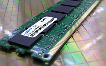
Mediante la combinazione di quattro chip di memoria DRAM DDR2, ciascuno dei quali con capacità di 512Mbit, Samsung è in grado di ottenere un package - wafer-level-processed stacked package (WSP) - con capacità complessiva di 2Gbit: l'impiego di due package di questo tipo sullo stesso PCB ha reso possibile la realizzazione di DIMM da 4 Gbit.
[Immagine ad alta risoluzione]

Samsung Electronics Co., Ltd., the world leader in advanced semiconductor technology solutions, today announced that it has developed the first all-DRAM stacked memory package using through silicon via (TSV) technology, which will soon result in memory packages that are faster, smaller and consume less power.
The new wafer-level-processed stacked package (WSP) consists of four 512 megabit (Mb) DDR2 (second generation, double data rate) DRAM (dynamic random access memory) chips that offer a combined 2 gigabits (Gb) of high density memory. Using the TSV-processed 2Gb DRAMs, Samsung can create a 4 GB (gigabyte) DIMM (dual in-line memory module) based on advanced WSP technology for the first time. Samsungs proprietary WSP technology not only reduces the overall package size, but also permits the chips to operate faster and use less power.
The innovative TSV-based MCP (multi-chip package) stacking technology offers next-generation packaging solution that will accommodate the ever-growing demand for smaller-sized, high-speed, high-density memory, said Tae-Gyeong Chung, vice president, Interconnect Technology Development Team, Memory Division, Samsung Electronics. In addition, the performance advancements achieved by our WSP technology can be utilized in many diverse combinations of semiconductor packaging, such as system-in-package solutions that combine logic with memory.
In todays MCPs, memory chips are connected by wire bonding, requiring vertical spacing between dies that is tens of microns deep. That wire bonding process also requires horizontal spacing on the package board hundreds of microns wide for the die-connecting wires. By contrast, Samsungs WSP technology forms laser-cut micron-sized holes that penetrate the silicon vertically to connect the memory circuits directly with a copper (Cu) filling, eliminating the need for gaps of extra space and wires protruding beyond the sides of the dies. These advantages permit Samsungs WSP to offer a significantly smaller footprint and thinner package.
Inside the new WSP, the TSV is housed within an aluminum (Al) pad to escape the performance-slow-down effect caused by the redistribution layer. Due to the complexity of DRAM stacking, this represented a much more difficult engineering feat than that accomplished with the first WSP, announced last year involving NAND flash dies.
There has been considerable concern that MCPs with high-speed memory chips with speed of 1.6Gb/ps next generation DRAM, would suffer from performance limitations when connected using current technologies. Samsungs WSP technology resolves these concerns.
In addition, as the back side of the wafer is ground away to make a thinner stack of multiple dies, the wafer has had a tendency to curve, creating physical distortion in the die. To overcome this additional critical concern in designing low-profile, high-density MCPs containing DRAM circuitry, Samsungs proprietary wafer-thinning technology, announced last year, has been applied to improve the thin-die-cutting process.
Advanced package solutions are increasingly important requirements for enabling high-speed, high-density memory solutions. Samsungs new stacked package design supports the rapid industry demand for high density, high performance semiconductor solutions that will support next-generation computing systems in 2010 and beyond.
News Source: Samsung Press Release
Links

![[Immagine ad alta risoluzione]](/images/?object=news4867_1.jpg)